|
Wafer Thinning |
|||||||||||||||||||||||||||||||||||||
|
|
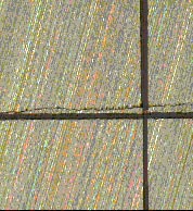
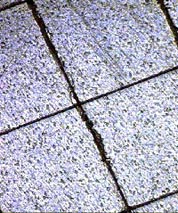
CHIPS' thinning process induces less stress in the wafer as opposed to standard backgrinding, which stress analysis indicates may induce stress over 70% of the wafer. Wafers thinned for CHIPS feature lower stress levels allowing for higher yields. Available finishes are #350-#2000. Limitations on standard thin is 152.4 microns (6 mils) for 6" and 8" wafers, both bumped and non-bumped. TTV is typically 0.6 microns.
|
|||||||||||||||||||||||||||||||||||||


